Introduction
The semiconductor industry stands at a critical inflection point in 2025 as Moore’s Law approaches physical limits. Two transformative trends are redefining chip manufacturing: chiplet-based architectures and the transition to 2nm process nodes. Together, they promise to deliver unprecedented performance while solving the industry’s most pressing challenges in power efficiency, cost, and design complexity.
This comprehensive 3,500-word analysis explores:
✔ How chiplet technology is disrupting traditional SoC designs
✔ The global race to 2nm production and key players
✔ Emerging applications from AI to quantum computing
✔ Geopolitical and supply chain implications
1. The Chiplet Revolution: Redefining Semiconductor Design
A. Why Chiplets? The End of Monolithic SoCs
Traditional system-on-chip (SoC) designs face three fundamental challenges:
- Yield collapse at advanced nodes (defect rates >30% at 3nm)
- Exponentially rising costs ($500M+ for 3nm mask sets)
- Physical limitations of die shrinking
Chiplets solve these through:
- Heterogeneous integration of specialized dies
- Advanced packaging (2.5D/3D, CoWoS, Foveros)
- Mix-and-match node combinations
B. Key Chiplet Architectures Compared
| Technology | Key Players | Advantages | 2025 Status |
|---|---|---|---|
| AMD’s Infinity | AMD, Xilinx | High bandwidth memory | Production-ready |
| Intel’s EMIB | Intel | Low latency interconnect | Scaling to 2nm |
| TSMC’s CoWoS | TSMC, NVIDIA | AI accelerator optimized | 2025 mass production |
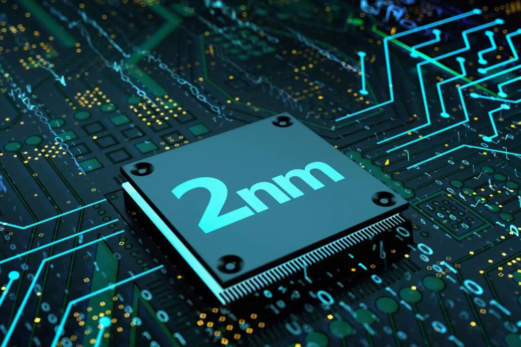
2. The 2nm Arms Race: Who’s Leading in 2025?
A. Process Node Roadmap
| Company | 2nm Timeline | Innovation | First Applications |
|---|---|---|---|
| TSMC | Late 2025 | Nanosheet GAA transistors | Apple A19, NVIDIA B100 |
| Samsung | Early 2025 | MBCFET technology | Galaxy S25, AI processors |
| Intel | Mid-2026 | RibbonFET + PowerVia | Data center CPUs |
B. Performance Projections at 2nm
- 15-20% speed boost vs 3nm at same power
- 30% power reduction at matched performance
- >50B transistors/cm² density
3. 2025 Applications: Where Chiplets and 2nm Collide
A. AI/ML Acceleration
- Modular AI chips combining:
- 2nm logic chiplets (NVIDIA)
- 3D-stacked HBM memory (SK Hynix)
- Optical I/O chiplets (Ayar Labs)
B. Next-Gen Consumer Devices
- iPhone 17 Pro: 2nm A19 chip with neural engine chiplets
- Meta AR glasses: 3D-integrated display/processor stack
C. Quantum-Hybrid Computing
- Cryogenic chiplets controlling qubits (Intel’s Horse Ridge III)
4. Challenges and Bottlenecks
A. Technical Hurdles
- Thermal management in 3D stacks (>500W/cm²)
- Standardization wars (UCIe vs. BoW vs. OpenHBI)
- Test complexity for known-good-die (KGD) yields
B. Geopolitical Factors
- Export controls on advanced packaging equipment
- TSMC’s Arizona fab delays impacting US supply
- China’s chiplet push through Hygon and SMIC
5. The 2030 Outlook: Beyond 2nm
A. Emerging Technologies
- CFET transistors (complementary FET)
- Atomic channel materials (MoS₂, graphene)
- Chiplet-based neuromorphic computing
B. Economic Projections
- $50B+ chiplet market by 2030 (Yole Développement)
- 2nm wafer costs exceeding $30,000
Conclusion
The semiconductor industry’s dual transition to chiplets and 2nm nodes represents more than just technological evolution—it’s a complete paradigm shift in computing architecture. As 2025 unfolds, we’ll see:
✔ Fragmentation of Moore’s Law into heterogeneous scaling
✔ New business models (chiplet marketplaces, IP licensing)
✔ Geopolitical rebalancing of chip manufacturing power